- 您现在的位置:买卖IC网 > Sheet目录2009 > MAX152EPP+ (Maxim Integrated Products)IC ADC 8BIT 1UA PWR-DWN 20-DIP
_________________________________________________________________________________________
MAX152
+3V, 8-Bit ADC with 1A Power-Down
4
_______________________________________________________________________________________
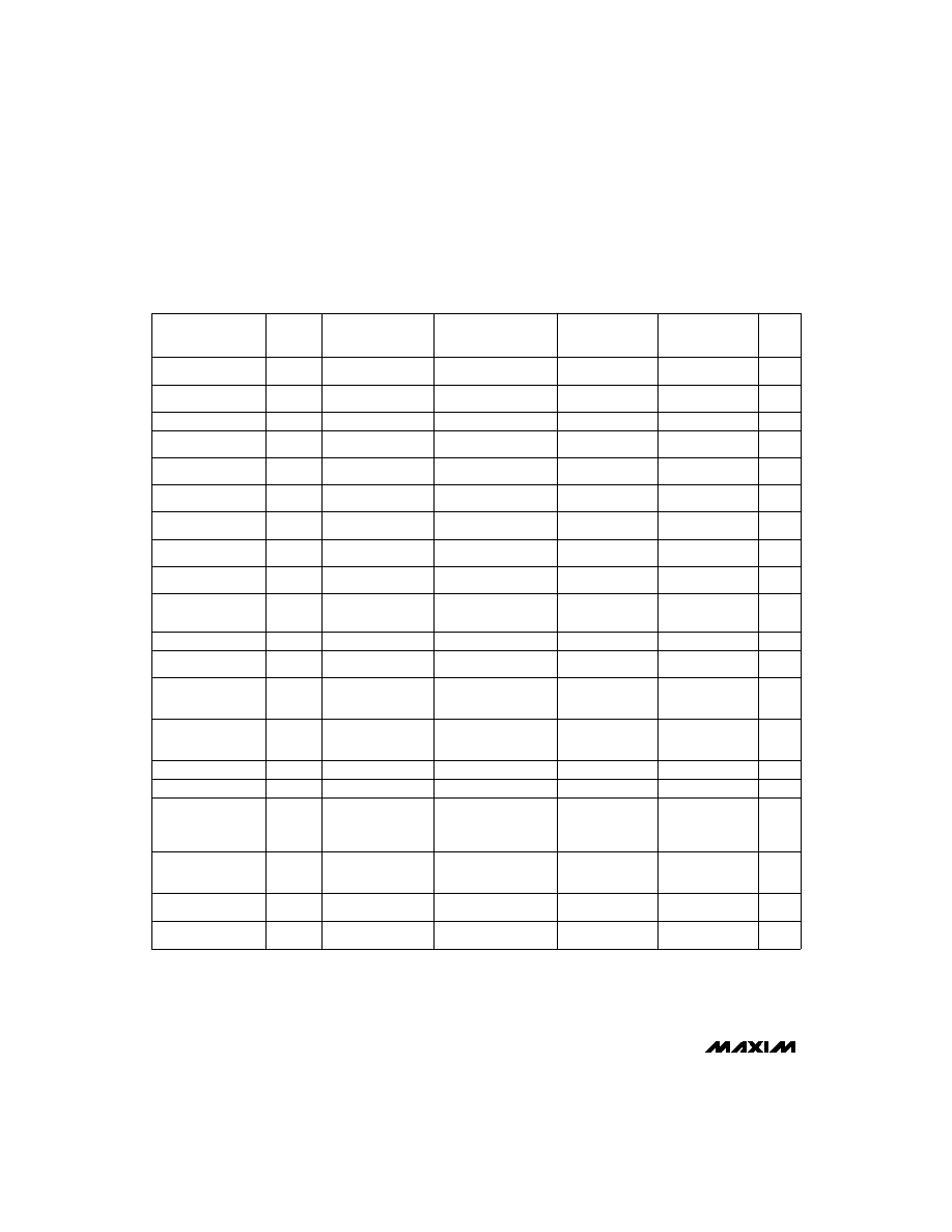
PARAMETER
SYMBOL
CONDITIONS
MAX152C/E
TA = TMIN to TMAX
MIN
MAX
MAX152M
TA = TMIN to TMAX
MIN
MAX
UNITS
WR Pulse Width
tWR
0.6
10
0.66
10
0.8
10
s
Delay Time Between
WR and RD Pulses
tRD
0.8
0.9
1.0
s
RD Pulse Width
tREAD1
400
500
600
ns
tACC1
400
500
600
ns
RD to INT Delay
tRI
300
340
400
ns
tCWR
tRD < tINTL,
CL = 100pF
1.8
2.06
2.4
s
Conversion Time
(RD Mode)
tCRD
2.0
2.3
2.6
s
Power-Up Time
tUP
0.9
1.2
1.4
s
CS to RD,WR
Setup Time
tCSS
0
ns
CS to RD,WR
Hold Time
tCSH
0
ns
CS to RDY
Delay
tRDY
CL = 50pF,
RL = 5.1k to VDD
100
120
140
ns
WR to INT Delay
tINTL
CL = 50pF
0.7
1.45
1.6
1.8
RD Pulse Width
tREAD2
WR-RD mode,
tRD > tINTL,
determined by tACC2
(Figure 5)
180
220
250
ns
Data Access Time
(Note 7)
tACC2
180
220
250
ns
WR to INT Delay
tIHWR
180
200
240
ns
Data Access Time
After
INT (Note 7)
tID
Stand-alone mode,
CL = 100pF
100
130
150
ns
Data Access Time
(RD Mode) (Note 7)
tACC0
CL = 100pF
tCRD
+100
tCRD
+150
ns
RD to INT Delay
(RD Mode)
tINTH
CL = 50pF
100
160
170
180
ns
Data Hold Time
(Note 8)
tDH
100
130
150
ns
tP
450
600
700
ns
ALL GRADES
TA = +25°C
MIN
TYP
MAX
Conversion Time
(WR-RD Mode)
Delay Time Between
Conversions
Data Access Time
(Note 7)
WR-RD mode,
determined by tACC1
(Figure 6)
WR-RD mode,
tRD < tINTL, CL = 100pF
(Figure 6)
WR-RD mode,
tRD < tINTL , CL = 100pF
(Figure 5)
tCRD
+130
s
TIMING CHARACTERISTICS
(Unipolar input range, VDD = 3V, VSS = 0V, TA = +25°C, unless otherwise noted.) (Note 6)
Note 6: Input control signals are specified with tr = tf = 5ns, 10% to 90% of +3.0V, and timed from a voltage level of 1.3V. Timing
delays get shorter at higher supply voltages. See the Converson Time vs. Supply Voltage graph in the
Typical Operating
Characteristics to extrapolate timing delays at other power-supply voltages.
Note 7: See Figure 1 for load circuit. Parameter defined as the time required for the output to cross 0.66V or 2.0V.
Note 8: See Figure 2 for load circuit. Parameter defined as the time required for the data lines to change 0.5V.
Stand-alone mode,
CL = 50pF
发布紧急采购,3分钟左右您将得到回复。
相关PDF资料
MAX153EPP+
IC ADC 8BIT 1MSPS HI-SPD 20-DIP
MAX154AENG+
IC ADC 8BIT 4CH W/MUX&REF 24-DIP
MAX155AEPI+
IC ADC 8BIT 8CH T/H&REF 28-DIP
MAX157AEUA+
IC ADC 10BIT 108KSPS 2CH 8-UMAX
MAX160CPN+
IC ADC 8BIT UP COMPATIBLE 18-DIP
MAX165ACPN+
IC ADC CMOS 8BIT UP COMP 18-DIP
MAX170CEPA+
IC ADC 12BIT SERIAL 8-DIP
MAX173CNG+
IC ADC 10BIT W/REF 24-DIP
相关代理商/技术参数
MAX152EVKIT-DIP
功能描述:数据转换 IC 开发工具 MAX152 Eval Kit RoHS:否 制造商:Texas Instruments 产品:Demonstration Kits 类型:ADC 工具用于评估:ADS130E08 接口类型:SPI 工作电源电压:- 6 V to + 6 V
MAX152EWP
功能描述:模数转换器 - ADC Integrated Circuits (ICs) RoHS:否 制造商:Texas Instruments 通道数量:2 结构:Sigma-Delta 转换速率:125 SPs to 8 KSPs 分辨率:24 bit 输入类型:Differential 信噪比:107 dB 接口类型:SPI 工作电源电压:1.7 V to 3.6 V, 2.7 V to 5.25 V 最大工作温度:+ 85 C 安装风格:SMD/SMT 封装 / 箱体:VQFN-32
MAX152EWP+
功能描述:模数转换器 - ADC 8-Bit 400ksps 3V Precision ADC RoHS:否 制造商:Texas Instruments 通道数量:2 结构:Sigma-Delta 转换速率:125 SPs to 8 KSPs 分辨率:24 bit 输入类型:Differential 信噪比:107 dB 接口类型:SPI 工作电源电压:1.7 V to 3.6 V, 2.7 V to 5.25 V 最大工作温度:+ 85 C 安装风格:SMD/SMT 封装 / 箱体:VQFN-32
MAX152EWP+T
功能描述:模数转换器 - ADC 8-Bit 400ksps 3V Precision ADC RoHS:否 制造商:Texas Instruments 通道数量:2 结构:Sigma-Delta 转换速率:125 SPs to 8 KSPs 分辨率:24 bit 输入类型:Differential 信噪比:107 dB 接口类型:SPI 工作电源电压:1.7 V to 3.6 V, 2.7 V to 5.25 V 最大工作温度:+ 85 C 安装风格:SMD/SMT 封装 / 箱体:VQFN-32
MAX152EWP-T
功能描述:模数转换器 - ADC RoHS:否 制造商:Texas Instruments 通道数量:2 结构:Sigma-Delta 转换速率:125 SPs to 8 KSPs 分辨率:24 bit 输入类型:Differential 信噪比:107 dB 接口类型:SPI 工作电源电压:1.7 V to 3.6 V, 2.7 V to 5.25 V 最大工作温度:+ 85 C 安装风格:SMD/SMT 封装 / 箱体:VQFN-32
MAX152MJP
功能描述:模数转换器 - ADC RoHS:否 制造商:Texas Instruments 通道数量:2 结构:Sigma-Delta 转换速率:125 SPs to 8 KSPs 分辨率:24 bit 输入类型:Differential 信噪比:107 dB 接口类型:SPI 工作电源电压:1.7 V to 3.6 V, 2.7 V to 5.25 V 最大工作温度:+ 85 C 安装风格:SMD/SMT 封装 / 箱体:VQFN-32
MAX15300ETI+
功能描述:DC/DC转换器 Auto-Comp digital PoL controller RoHS:否 制造商:Murata 产品: 输出功率: 输入电压范围:3.6 V to 5.5 V 输入电压(标称): 输出端数量:1 输出电压(通道 1):3.3 V 输出电流(通道 1):600 mA 输出电压(通道 2): 输出电流(通道 2): 安装风格:SMD/SMT 封装 / 箱体尺寸:
MAX15300ETI+T
功能描述:DC/DC转换器 Auto-Comp digital PoL controller RoHS:否 制造商:Murata 产品: 输出功率: 输入电压范围:3.6 V to 5.5 V 输入电压(标称): 输出端数量:1 输出电压(通道 1):3.3 V 输出电流(通道 1):600 mA 输出电压(通道 2): 输出电流(通道 2): 安装风格:SMD/SMT 封装 / 箱体尺寸: